Certaines informations sont présentées en anglais.
À propos de moi
My Expertise:
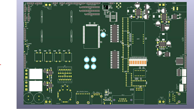
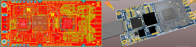
Complex Layouts: Multi-layer stacks (4-12+ layers), High-Speed Digital, RF, and Power Electronics.
Signal Integrity: Impedance matching, differential pairs, and EMI/EMC mitigation.
Software Proficiency: Altium Designer, KiCad, Eagle, EasyEDA.
Full Documentation: BOM optimization (Active component sourcing), Pick & Place, and Gerber fabrication files.
What I deliver:
Schematic Capture & Validation
PCB Layout (3D Modeling included)
Complete Fabrication Output (Gerber/NC Drill/BOM)
Engineering support to ensure your board works.
Do not risk your project with amateur errors.... Plus d’infos