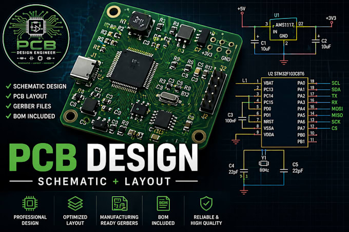
PCB Design Engineer, Schematic, Layout and Circuit Design
Royaume-Uni
Allemand, Français
Certaines informations sont présentées en anglais.
À propos de moi
I am a PCB Design Engineer specializing in schematic design, PCB layout, and circuit development for embedded systems, IoT devices, and electronic products. I create accurate schematics, optimized PCB layouts, and production-ready Gerber files using industry-standard tools such as Altium Designer and KiCad. My work focuses on signal integrity, efficient component placement, and manufacturable designs. I also provide support with BOM creation, circuit debugging, and design optimization to ensure reliable and cost-effective hardware solutions.... Plus d’infos