Parcourir les catégories
Explorer
Fiverr Pro
Français
$
USD
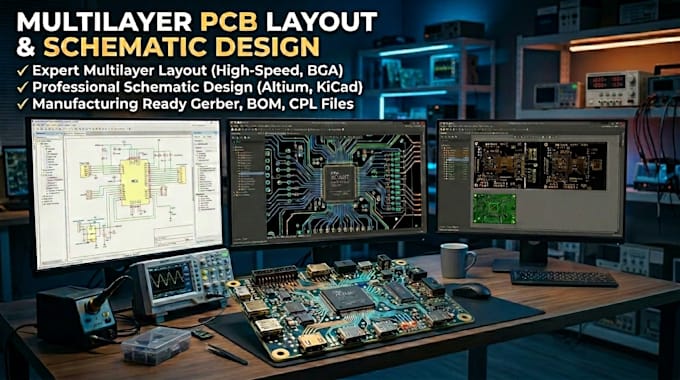
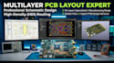
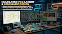
Multilayer PCB Expert
Building hardware is hard. If your layout isn't right, you deal with noise, heat, or boards that just don't work. I handle the heavy lifting of multilayer design so you can focus on your product. I've spent years turning messy breadboards into high-performance PCBs that actually pass testing.
Service Included:
I believe the best boards are designed with the manufacturer in mind. A beautiful layout is useless if the fab house can't build it reliably or cheaply.
How it works:
Send over your project details and let's get your board built.
Format de fichier:
Gerber
•
STEP
•
BRD
•
SCH
•
Logiciel:
Altium Designer
•
EasyEDA
•
Fusion 360
•
KiCad
Interface:
I2S
•
UART
•
USB
•
SPI
•
SDIO
•
Wi-Fi
•
BLE
•
Ethernet
What software do you use for the design?
I primarily use Altium Designer and KiCad. If you need the source files in a specific format, just let me know before we start.
Can you help me source components that are actually in stock?
Yes. I check real-time availability on Mouser and DigiKey to ensure the BOM doesn't include obsolete or out-of-stock parts.
Do you provide the manufacturing files?
Always. You will get a full production package including Gerbers, NC Drill files, Pick and Place data, and the BOM.