Parcourir les catégories
Explorer
Fiverr Pro
Français
$
USD
Embedded Systems and PCB Design Engineer
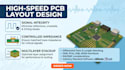
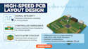
I will design high-speed PCB layouts with controlled impedance, signal integrity optimization, and professional routing techniques for advanced embedded systems, communication hardware, and high-frequency electronic products.
I specialize in multi-layer PCB design optimized for stable signal transmission, EMI reduction, power integrity, and manufacturing-ready performance.
My services include:
Why Choose Me?
Contact me before placing your order so we can discuss your PCB requirements, interface speeds, stackup constraints, and the best routing approach for your hardware project.
What do you need to start my high-speed PCB project?
Schematic, interface requirements, stackup details, target impedance, and any design constraints or reference files.
Can you handle controlled impedance routing?
Yes, I design impedance-controlled PCB layouts for high-speed and high-frequency applications.
Do you optimize signal integrity and EMI performance?
Yes, I focus on signal integrity, differential pair matching, and EMI reduction techniques.
Which high-speed interfaces do you support?
I support USB, HDMI, PCIe, Ethernet, DDR, SPI, I2C, UART, and other high-speed interfaces.
Will I receive manufacturing-ready PCB files?
Yes, you will receive Gerber files, BOM, and complete production-ready documentation.


