Parcourir les catégories
Explorer
Fiverr Pro
Français
$
USD
Technicien en électronique Développeur frontend
VEUILLEZ ME CONTACTER AVANT DE PASSER COMMANDE
Pour garantir les meilleurs résultats et confirmer la complexité du projet, veuillez m’envoyer un message avec vos exigences avant de commander. Assurons-nous d’être sur la même longueur d’onde !
Ce que je propose dans ce service :
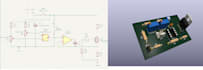
Capture schématique (si vous choisissez le service supplémentaire)
Routage et optimisation du layout pour PCB 1 ou 2 couches
Attribution des footprints et création de composants personnalisés si nécessaire
Liste de matériaux (BOM) avec détails des composants
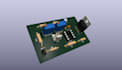
Modèle 3D de votre carte finie (.STEP ou images en vue 3D)
Fichiers Gerber prêts pour la production (compatibles avec JLCPCB, PCBWay, etc.)
Idéal pour :
Projets Arduino, ESP32 et microcontrôleurs en général
Cartes de capteurs et électroniques DIY modulaires
Projets de laboratoire étudiant et petits circuits d’automatisation
Prototypage et créations pour hobbyistes
Mon objectif principal est de fournir un routage propre, des plans de masse adéquats et une documentation précise.
Envoyez-moi un message avec votre schéma,

Format de fichier:
Gerber
•
BRD
•
SCH
•
•
Autres
Logiciel:
KiCad
Interface:
UART
•
USB
•
SPI
•
I2C


