Parcourir les catégories
Explorer
Fiverr Pro
Français
$
USD
Ingénieur professionnel en électricité et électronique
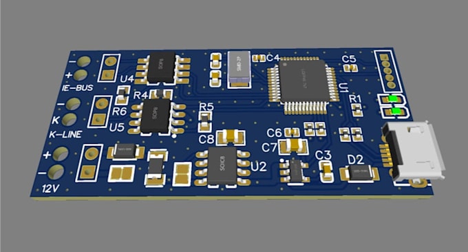
Vous avez besoin d'une conception avancée de PCB multicouche, d'un agencement PCB et d'un Altium PCB optimisé pour la fabrication ?
Je fournis des cartes propres, efficaces et prêtes pour la production avec de bonnes performances et fiabilité en utilisant Altium Designer, KiCad, et EasyEDA.
Je me concentre sur des conceptions multicouches de haute qualité avec un routage approprié, l'intégrité du signal et une analyse DFM pour garantir que votre PCB fonctionne parfaitement et est prêt pour la fabrication.
Ce que je propose :
Logiciels :
Altium Designer, KiCad, EasyEDA
Fichiers que vous recevrez :
Avantages :
CONTACTEZ-NOUS MAINTENANT ! commençons.
Spécialisation:
Conception de circuit
•
Schémas
•
Mise en page
•
Gerber
Format de fichier:
Gerber
•
3DS
•
Logiciel:
Allegro
•
Altium Designer
•
Eagle CAD
•
EasyEDA
•
KiCad
•
Proteus
Traduction automatique
Quels détails avez-vous besoin pour commencer ma conception de PCB ?
J'ai besoin de votre schéma électrique, taille de la carte, nombre de couches, liste des composants (BOM), et toute exigence spécifique comme le contrôle d'impédance ou signaux à haute vitesse.
Concevez-vous des PCBs multicouche et à haute vitesse ?
Oui. Je conçois des PCBs multicouches, y compris des designs à haute vitesse avec un routage, une mise à la masse et une intégrité du signal appropriés.
Quel logiciel utilisez-vous pour la conception de PCB ?
J'utilise Altium Designer pour la conception professionnelle de PCB, ainsi que d'autres outils si nécessaire pour des tâches spécifiques.
Mon PCB sera-t-il prêt pour la fabrication ?
Oui. Vous recevrez des fichiers Gerber, des fichiers de perçage, et des fichiers prêts pour la fabrication optimisés avec une analyse DFM.
Effectuez-vous des vérifications DFM (Design for Manufacturing) ?
Oui. Je m'assure que votre conception de PCB passe l'analyse DFM, réduisant ainsi les erreurs de fabrication et améliorant la fiabilité.
Pouvez-vous améliorer ou optimiser une conception de PCB existante ?
Oui. Je peux analyser, redessiner et optimiser votre PCB pour de meilleures performances, un routage amélioré et une meilleure fabricabilité.
Gérez-vous le placement des composants et l'optimisation du routage ?
Oui. Je fournis un placement optimisé des composants et un routage propre pour une performance électrique efficace et un design compact.
Pouvez-vous concevoir des PCBs pour des applications spécifiques comme IoT ou systèmes embarqués ?
Oui. Je conçois des PCBs pour des dispositifs IoT, des systèmes embarqués, de la robotique et des produits électroniques.