Parcourir les catégories
Explorer
Fiverr Pro
Français
$
USD
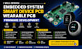
Expert PCB Designer Schematics Layouts and Prototype Solutions
Hello welcome!
Bring your electronics projects to life! I specialize in designing PCBs for embedded systems, smart devices, wearables, and firmware development. My goal is to provide precise, manufacturable, and high-performance PCB solutions tailored to your needs.
What I Offer:
Why Choose Me:
Contact me today and lets start building your next electronics project!


What information do you need to start designing my PCB?
I need your schematic, circuit diagram, project requirements, and any preferred components or board size.
Do you provide Gerber files ready for manufacturing?
Yes, all packages include Gerber files and BOMs ready for fabrication.
Can you design multi-layer or complex PCBs?
Absolutely! My standard and premium packages cover multi-layer, IoT, wearable, and embedded system PCBs.
Do you offer firmware integration or testing?
Yes, all packages include Gerber files and BOMs ready for fabrication.
How long will it take to complete my PCB design?
Delivery depends on the package: Basic – 4 days, Standard – 7 days, Premium – 10 days. Expedited delivery is also available.


