Certaines informations sont présentées en anglais.
À propos de moi
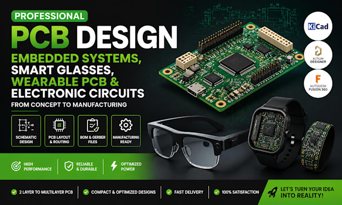
I am a professional PCB Design Engineer specializing in PCB layout, schematic design, and electronic hardware development. I help startups, engineers, and businesses turn their ideas into reliable, production-ready circuit boards. My expertise includes 2-layer and multilayer PCB design, component placement, signal routing, Gerber file generation, BOM creation, DRC checking, and design optimization. I work with tools like KiCad and Altium Designer to deliver high-quality PCB solutions for IoT devices, embedded systems, sensors, and custom electronics with accuracy and attention to detail.... Plus d’infos