Parcourir les catégories
Explorer
Fiverr Pro
Français
$
USD
Ingénieur Interface RF, réseau sans fil, Ethernet, CAN, PCB haute vitesse
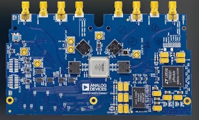
Need a custom PCB for wireless connectivity or industrial communication? Our engineering team develops schematics and board layouts for IoT products, sensors and embedded systems.
We work with module-based Wi-Fi, BLE, LoRa, cellular and GNSS designs, alongside Ethernet, CAN and RS-485 circuits. Before starting, we confirm your selected components, technical requirements and project scope.
Deliverables include:
Our design process considers RF routing, antenna clearance, grounding, power distribution and signal return paths.
Basic includes layout from your approved schematic. Standard adds circuit design. Premium covers two agreed communication circuits and a bring-up checklist.
Firmware, fabrication, assembly, lab testing and certification are excluded.
Send our team your specifications and board dimensions before ordering to confirm scope.


Traduction automatique
Cette prestation est-elle réalisée par une équipe ?
Oui. Notre équipe d’ingénierie gère votre périmètre de schéma et de conception PCB convenu. Vous bénéficiez d’une communication coordonnée et d’un ensemble consolidé de livrables du projet.
En quoi cela diffère-t-il de votre service de révision de conception ?
Ce service crée un nouveau schéma ou un layout PCB dans le cadre convenu. Notre service de révision évalue une conception existante et fournit des conclusions et des recommandations sans créer ni modifier le PCB.
Votre équipe peut-elle concevoir à la fois des interfaces sans fil et filaires ?
Notre périmètre indiqué inclut des circuits modulaires Wi‑Fi, BLE, LoRa, cellulaire et GNSS, ainsi que des interfaces Ethernet, CAN et RS-485. Envoyez d’abord les détails de vos composants pour que nous puissions confirmer la compatibilité avec nos capacités.
Quels fichiers allons-nous recevoir ?
Selon votre package, vous recevez les exports de fabrication du PCB, des fichiers de conception modifiables, un schéma et une nomenclature. Nous convenons au préalable du logiciel de CAO, des formats de fichier et des sorties de fabrication avant le début des travaux.
La commande inclut-elle un prototype fonctionnel ou une certification ?
Non. Ce service livre des fichiers de conception, et non du matériel assemblé ni une performance certifiée. La fabrication, l’assemblage, le firmware, les tests physiques et la certification sont des activités distinctes. Nous pouvons documenter les hypothèses de conception et les étapes de test convenues.