Parcourir les catégories
Explorer
Fiverr Pro
Français
$
USD
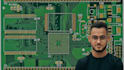
Power Electronics, IoT PCB Design, Embedded and High Speed Systems
Building a high speed digital product and need a PCB layout that performs reliably beyond basic routing?
I specialize in multilayer PCB design with a strong focus on signal integrity, impedance control, and manufacturing readiness.
From embedded systems and IoT devices to communication, industrial, and high performance electronics, I create PCB layouts that minimize noise, reduce signal loss, and support stable operation at high data rates.
What you can expect:
I work with Altium Designer, KiCad, EasyEDA, OrCAD, Eagle, and other industry standard tools.
Every project is approached with performance, reliability, and production in mindhelping you move from concept to fabrication with confidence. NDA friendly and committed to protecting your intellectual property.