Certaines informations sont présentées en anglais.
À propos de moi
welcome to my profile
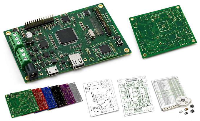
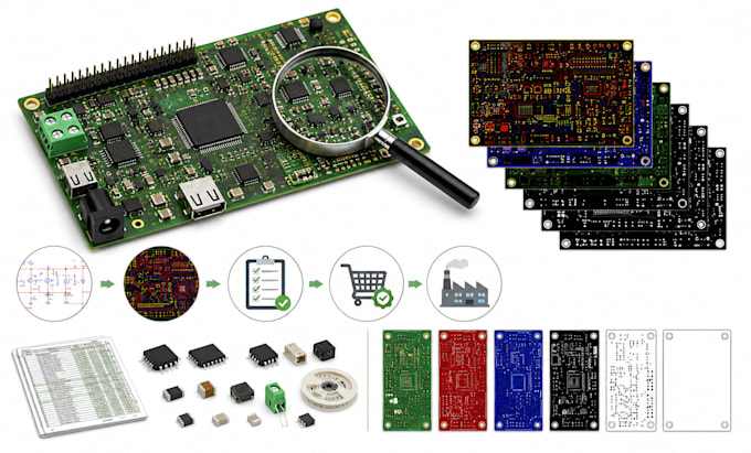
I am a professional PCB Design Engineer specializing in high-quality PCB layout using Altium Designer and KiCad. I provide schematic capture, multilayer PCB design, high-speed routing, signal and power integrity optimization, DFM review, Gerber generation, BOM creation, and manufacturing-ready documentation. My goal is to deliver reliable, production-ready PCB solutions with precision, fast turnaround, and excellent communication for every project.
thanks
... Plus d’infos