Certaines informations sont présentées en anglais.
À propos de moi
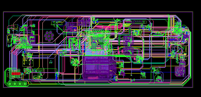
I am an Electronics and Communication Engineering graduate with hands-on experience in PCB design using Cadence OrCAD Capture and Allegro PCB Designer. I specialize in 16-layer PCB layouts, footprint creation, and differential pair routing. I am seeking a Junior PCB Design Engineer role to contribute to innovative hardware development projects.... Plus d’infos