Parcourir les catégories
Explorer
Fiverr Pro
Français
$
USD
INGÉNIEUR ÉLECTRONIQUE ET ÉLECTRIQUE
Je concevrai et développerai schéma PCB, RF PCB et layout PCB haute vitesse avec précision professionnelle et respect des normes de fabrication.
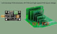
Je me spécialise dans la transformation de vos idées électroniques en designs PCB entièrement fonctionnels et prêts pour la production pour des dispositifs IoT, systèmes embarqués, communication sans fil et circuits numériques haute vitesse.
En utilisant des outils avancés comme Altium Designer, Cadence OrCAD, Allegro et KiCad, je fournis des schémas clairs, des layouts PCB optimisés et un routage précis qui garantissent une forte intégrité du signal et une performance stable du circuit.
Je résous des problèmes critiques de PCB tels que interférences de bruit, distorsion du signal, instabilité RF, routage inadéquat, connexions schématiques incorrectes et perte de données à haute vitesse en appliquant des règles d’ingénierie appropriées et les meilleures pratiques de conception.
Vous recevrez les fichiers complets du schéma PCB (SCH), le design du layout PCB, les fichiers Gerber pour la fabrication, le modèle STEP 3D pour l’assemblage mécanique et la documentation PDF pour la revue.
Mon service vise à fournir des designs PCB sans erreur, optimisés et prêts pour la fabrication adaptés aussi bien aux projets simples qu’aux projets complexes incluant RF et applications haute vitesse.
Je m’assure que chaque design est propre et précis
CONTACTEZ-MOI MAINTENANT

Traduction automatique
Fournissez-vous des PCB prêts pour la fabrication ?
Oui. Je fournis des fichiers entièrement prêts pour la fabrication, y compris Gerber, layout PCB et schéma, garantissant que votre design peut être envoyé directement à la fabrication sans erreurs ni données manquantes.
Pouvez-vous gérer la conception de PCB RF et haute vitesse ?
Oui. Je me spécialise dans la conception de PCB RF et haute vitesse, en appliquant un contrôle d’impédance approprié, des techniques d’intégrité du signal et des méthodes de réduction du bruit pour une performance stable.
Et si je n'ai qu'une idée et pas de schéma ?
Pas de problème. Je peux transformer votre idée en un schéma professionnel complet et un design PCB, en vous guidant du concept aux fichiers finaux de fabrication.
Ma conception de PCB sera-t-elle sans erreur ?
Oui. Je réalise des vérifications pour détecter courts-circuits, erreurs de routage, interférences de signal et problèmes de placement des composants afin d’assurer un design propre et fiable.
Quels fichiers vais-je recevoir à la fin ?
Vous recevrez des fichiers Gerber, le layout PCB, les fichiers schéma (SCH), le modèle STEP 3D et la documentation PDF, tous prêts pour la production et la revue.
