Parcourir les catégories
Explorer
Fiverr Pro
Français
$
USD
CONCEPTION DE PCB
Bonjour,
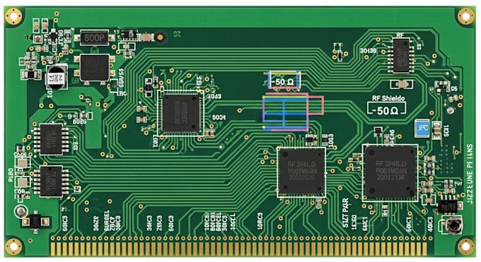
Concevoir des circuits RF pour l’électronique moderne est un équilibre délicat entre performance du signal, contraintes de taille et faisabilité de fabrication.
Je propose des services professionnels de layout de PCB RF utilisant la technologie HDI (High-Density Interconnect) et le routing à impedance contrôlée pour garantir la performance fiable de vos designs à haute fréquence.
Services que je propose
Pourquoi travailler avec moi
Logiciels & outils
Contactez-moi avant de commander pour discuter de vos besoins en layout RF, HDI et impedance afin que nous puissions créer un PCB haute performance et prêt pour la production.
Traduction automatique
Pouvez-vous gérer des layouts HDI denses ?
Oui, je suis spécialisé dans les layouts de PCB RF à haute densité avec microvias.
Les signaux maintiendront-ils une impedance correcte ?
Absolument. Le routing à impedance contrôlée est appliqué à toutes les traces à haute vitesse.
Les designs sont-ils prêts pour la production ?
Oui, tous les PCBs sont vérifiés DFM et prêts pour la fabrication et l'assemblage.