Parcourir les catégories
Explorer
Fiverr Pro
Français
$
USD
Ingénieur en systèmes embarqués et conception PCB, expert en Altium, KiCad, EasyEDA
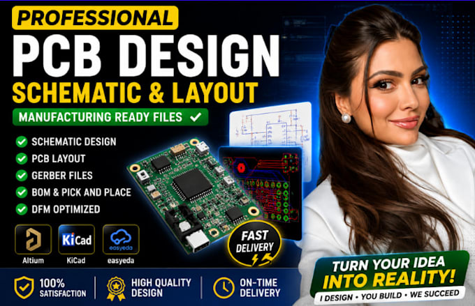
CONCEVOIR SCHÉMA ET LAYOUT PCB, FICHIERS GERBER PRÊTS POUR LA FABRICATION, BOM, EMPREINTES
Vous avez besoin d’un design PCB professionnel prêt pour la fabrication ?
Je concevrai un layout PCB de haute qualité, un schéma, et des fichiers prêts pour la fabrication pour votre projet électronique en utilisant EasyEDA, KiCad ou Altium Designer.
MES SERVICES INCLUENT :
PROJETS SUPPORTÉS :
VOUS RECEVREZ :
POURQUOI ME CHOISIR ?
Veuillez me contacter avant de passer commande pour discuter de vos besoins en projet.
Traduction automatique
Quel logiciel de PCB utilisez-vous ?
Je travaille avec Altium Designer, KiCad et EasyEDA
Pouvez-vous créer le schéma à partir de mon idée ?
Oui. Je peux concevoir le schéma complet selon vos exigences.
Vais-je recevoir les fichiers Gerber ?
Oui. Les fichiers Gerber sont inclus dans tous les packages.
Pouvez-vous redessiner un PCB existant ?
Oui. Je peux modifier, optimiser ou redessiner des projets PCB existants.
La conception est-elle prête pour la fabrication ?
Oui. Tous les fichiers livrés sont préparés pour la fabrication PCB.
Pouvez-vous aider avec des projets ESP32, STM32 ou Arduino ?
Oui. Ces plateformes font partie de mes spécialités principales.