Parcourir les catégories
Explorer
Fiverr Pro
Français
$
USD

Expertise in AI Hardware Acceerator, ASIC, FPGA, RISC V, Embedded system
Compétences
Voir mes services
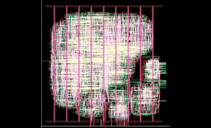

Lead ASIC Design Engineer & Chip Architect
LightRail AI
Jul 2026 - Present • 3 mos
As Lead ASIC Design Engineer & Chip Architect, I led the end-to-end development of a multi-precision Neural Compute Accelerator, taking the design from architecture and RTL through physical implementation and final chip-level GDSII. I defined and integrated the accelerator architecture around INT8, BF16, BF24, and FP32 accumulation, using shared compute resources, SIMD processing, systolic/tiled GEMM execution, convolution support, tensor/register storage, and an AXI4-Lite control interface. My responsibilities included RTL architecture, datapath design, verification, synthesis, timing analysis, floorplanning, placement, routing, hierarchical hard-macro integration, IO padframe construction, power distribution, chip-level routing, density fill, and final GDSII assembly using the SkyWater SKY130 130 nm process. The final chip implementation includes an 8.2 mm × 8.2 mm die, a 6.525 mm × 6.525 mm hardened accelerator core, 154 signal GPIO pads, 16 power/ground pads, and a complete IO ring. The routed design contains approximately 1.044 m of interconnect and 5,999 vias, with zero detailed-routing violations in the completed OpenROAD routing stage. This role involved both chip architecture and physical-design leadership, requiring decisions across compute architecture, mixed-precision arithmetic, timing closure, hierarchical integration, IO planning, PDN design, and fabrication-oriented GDSII handoff.
