Parcourir les catégories
Explorer
Fiverr Pro
Français
$
USD
Ingénieur en conception de circuits imprimés
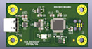
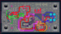
Fort d'une vaste expérience en ingénierie électronique, je combine expertise technique et passion pour l'innovation. Ma spécialisation dans la conception de PCB et le développement de firmware me permet de fournir des solutions fiables et de haute qualité, adaptées aux besoins du client. Qu'il s'agisse de systèmes embarqués, d'appareils IoT ou de projets de communication sans fil, je me concentre sur la création de designs efficaces et pratiques avec professionnalisme et souci du détail. Je suis dédié à donner vie à vos idées et à assurer que votre projet obtienne les meilleurs résultats possibles.
Ce que je propose
Pourquoi me choisir ?

Format de fichier:
Gerber
•
STEP
•
SCH
•
•
ODB
Logiciel:
EasyEDA
•
KiCad
Interface:
HDMI
•
UART
•
USB
•
I2C
•
Wi-Fi
•
BLE
•
BT
•
LTE
Traduction automatique
J'ai une conception de circuit, pouvez-vous la convertir en disposition de PCB
Oui, je peux créer un layout PCB professionnel pour votre projet basé sur le schéma que vous fournissez.
J'ai une idée de projet, pouvez-vous concevoir le schéma et le PCB pour cela ?
Oui, je peux vous aider à ce sujet. Veuillez décrire votre idée de projet en détail, y compris ce que vous souhaitez que le système accomplisse.
Proposez-vous des révisions ?
Oui, je propose des révisions gratuites en fonction du package choisi pour m'assurer que vous êtes entièrement satisfait du design final.
Allez-vous signer un accord de confidentialité ?
Oui, je suis disposé à signer un accord de non-divulgation (NDA) pour garantir que les détails de votre projet restent entièrement confidentiels.


