Parcourir les catégories
Explorer
Fiverr Pro
Français
$
USD
Concepteur de PCB et développeur de systèmes embarqués, solutions industrielles et IoT, KiCad
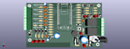
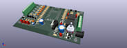
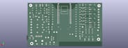
Vous avez déjà réalisé la partie la plus difficile, le schéma est prêt. Maintenant, vous avez besoin d’un layout PCB propre et fabriquable qui fonctionne réellement.
Je prendrai votre schéma et le transformerai en un layout KiCad professionnel : placement correct des composants, routage propre, validation des règles de conception et fichiers Gerber prêts à la fabrication que vous pouvez envoyer directement à n’importe quel fabricant.
Ce que vous obtenez :
Placement organisé des composants pour le flux de signal et la gestion thermique
Routage propre avec des largeurs de traces et des espacements appropriés
Validation complète DRC sans erreurs ni surprises chez le fabricant
Fichiers Gerber compatibles avec JLCPCB, PCBWay et toute autre usine de fabrication
Délais rapides, communication claire et fichiers prêts à être fabriqués dès le premier jour.
Envoyez-moi votre schéma et réalisons votre carte.
Format de fichier:
Gerber
•
STEP
•
SCH
•
3DS
•
Logiciel:
KiCad
Interface:
I2S
•
UART
•
USB
•
SPI
•
I2C
•
SDIO
•
Wi-Fi
•
BLE
•
BT
Traduction automatique
Dans quel format dois-je envoyer mon schéma ?
Le format KiCad est préféré. J’accepte aussi les schémas PDF ou autres formats — contactez-moi avant de commander si vous n’êtes pas sûr.
Que faire si mon schéma comporte des erreurs ?
Si je trouve des erreurs lors du layout, je vous en informerai immédiatement avant de continuer. Des corrections du schéma peuvent être ajoutées en tant qu’offre personnalisée si nécessaire.
Les fichiers Gerber sont-ils compatibles avec n’importe quel fabricant ?
Oui. Tous les fichiers respectent les spécifications standard de fabrication et fonctionnent avec JLCPCB, PCBWay, OSHPark et toute autre usine de fabrication dans le monde.
Pouvez-vous aussi concevoir le schéma à partir de zéro ?
Ce service couvre uniquement le layout. Pour une capture complète du schéma et le layout ensemble, consultez mes autres services ou contactez-moi pour une offre personnalisée.
Et si j’ai besoin de plus de composants que la limite du package ?
Des composants supplémentaires peuvent être achetés en option. Contactez-moi avant de commander si votre conception dépasse largement la limite du package.


