Parcourir les catégories
Explorer
Fiverr Pro
Français
$
USD

PLEASE CONTACT ME BEFORE PLACING AN ORDER!
TECHNICAL NOTICE: RF and High-Speed designs require extreme precision. Please provide your Schematic, Stack-up requirements (if any), and Target Impedance values. Contact me first for a free preliminary review to ensure your project meets industrial SI/PI (Signal & Power Integrity) standards.
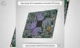
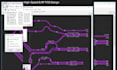
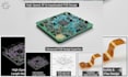
High-Speed, RF & Impedance Controlled PCB Design
Are you dealing with signal integrity issues, EMI/EMC challenges, or complex RF requirements? I specialize in advanced PCB layouts where precision is not an option, but a necessity.
My Expertise Includes:
Veuillez informer le freelance de toute préférence ou préoccupation concernant l'utilisation d'outils d'IA dans la réalisation et/ou la livraison de votre commande.
LoRaWAN Industrial Solution, PCB Design, SEO and Cybersecurity
Langues
How do you guarantee signal integrity in your designs?
I follow strict design rules for high-speed routing, including differential pair matching, length tuning (meandering), and controlled impedance. I also design specific stack-ups to minimize crosstalk and EMI, ensuring your board meets all functional and certification requirements.
Can you design PCBs for RF protocols like WiFi, LoRa, or Bluetooth?
Yes. I have extensive experience in RF layout, including antenna integration, matching networks (Pi-networks), and ground plane optimization to maximize range and minimize signal loss.
Do you provide the stack-up details for controlled impedance?
Absolutely. I provide a detailed layer stack-up report that you can send directly to your manufacturer. This includes dielectric constants (Dk), copper weights, and trace widths calculated for your specific impedance requirements (e.g., 50 ohm single-ended or 90/100 ohm differential).
Can you handle complex BGA and FPGA routing?
Yes, I specialize in High-Density Interconnect (HDI) designs involving fine-pitch BGA components, utilizing blind and buried vias or via-in-pad technology when necessary to ensure clean breakout and routing.
What information do you need for an RF or High-Speed project?
Beyond the schematic, I need to know the target operating frequencies, specific interface standards (e.g., USB 3.0, DDR4), and if possible, your preferred PCB manufacturer’s capabilities to ensure the design is production-ready.
Do you offer EMI/EMC optimization?
Yes. I implement shielding techniques, proper decoupling capacitor placement, and solid return path planning to reduce electromagnetic interference and help your product pass EMC testing.
Do you work with a team?
Yes, I work with a team of experienced engineers to ensure that every project passes DFM (Design for Manufacturing) checks and is ready for industrial production.


