Circuit Board Designer PCB Layout, DFM and High Speed Routing
États-Unis
Anglais
Certaines informations sont présentées en anglais.
À propos de moi
I design printed circuit boards on screen, from schematic to fabrication-ready files. Each project is checked against your design rules and your fabricator’s limits before delivery.
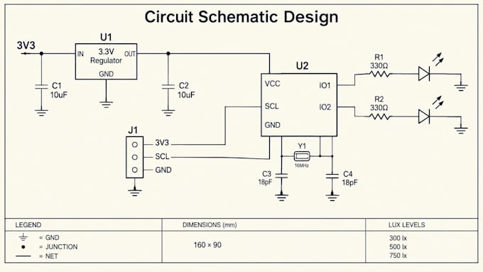
• Schematic capture and part selection
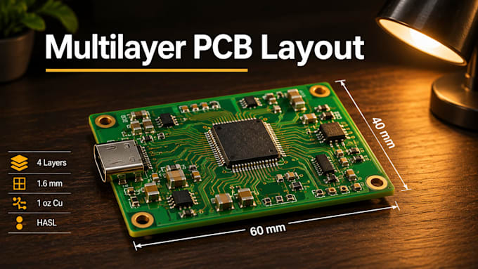
• Multilayer PCB layout and routing
• High speed routing with impedance control
• DFM checks, Gerber, BOM and pick and place files
Tools: Altium Designer, KiCad, OrCAD, Excel, a Gerber viewer.
Send your schematic or specs before ordering and I will confirm scope and price.... Plus d’infos