Parcourir les catégories
Explorer
Fiverr Pro
Français
$
USD
JLC PCB
About this gig
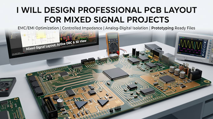
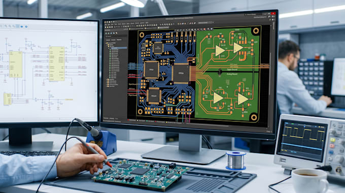
I design professional mixed signal PCB layouts for analog, digital, RF, power, and embedded systems. I deliver clean, optimized, and manufacturing ready PCB designs using Altium Designer, KiCad, and EasyEDA.
What I Offer
Why Choose Me
Services Included
Contact me today with your project details and lets create a reliable, efficient, and manufacturing ready PCB solution for your product.


Spécialisation:
Conception de circuit
•
Schémas
•
Mise en page
Format de fichier:
Gerber
•
BRD
•
Logiciel:
Altium Designer
•
Eagle CAD
•
KiCad
Interface:
HDMI
•
I2S
•
I2C
•
Wi-Fi
•
BLE
•
BT
What software do you use for PCB design?
I mainly use Altium Designer, KiCad, and EasyEDA depending on your project needs.
Can you design both schematic and PCB layout?
Yes, I can handle complete PCB development from schematic capture to final manufacturing files.
Will I receive manufacturing files?
Absolutely. You will receive Gerber files, BOM, Pick and Place files, PDF schematics, and all source files.
Can you work on high speed or RF designs?
Yes, I have experience with mixed signal, RF, high speed, and embedded PCB projects requiring signal integrity and EMI optimization.